- 您现在的位置:买卖IC网 > Sheet目录3893 > PIC16F723A-I/SS (Microchip Technology)MCU PIC 7KB FLASH XLP 28-SSOP
PIC16(L)F722A/723A
DS41417B-page 214
2010-2012 Microchip Technology Inc.
TABLE 23-3:
CLKOUT AND I/O TIMING PARAMETERS
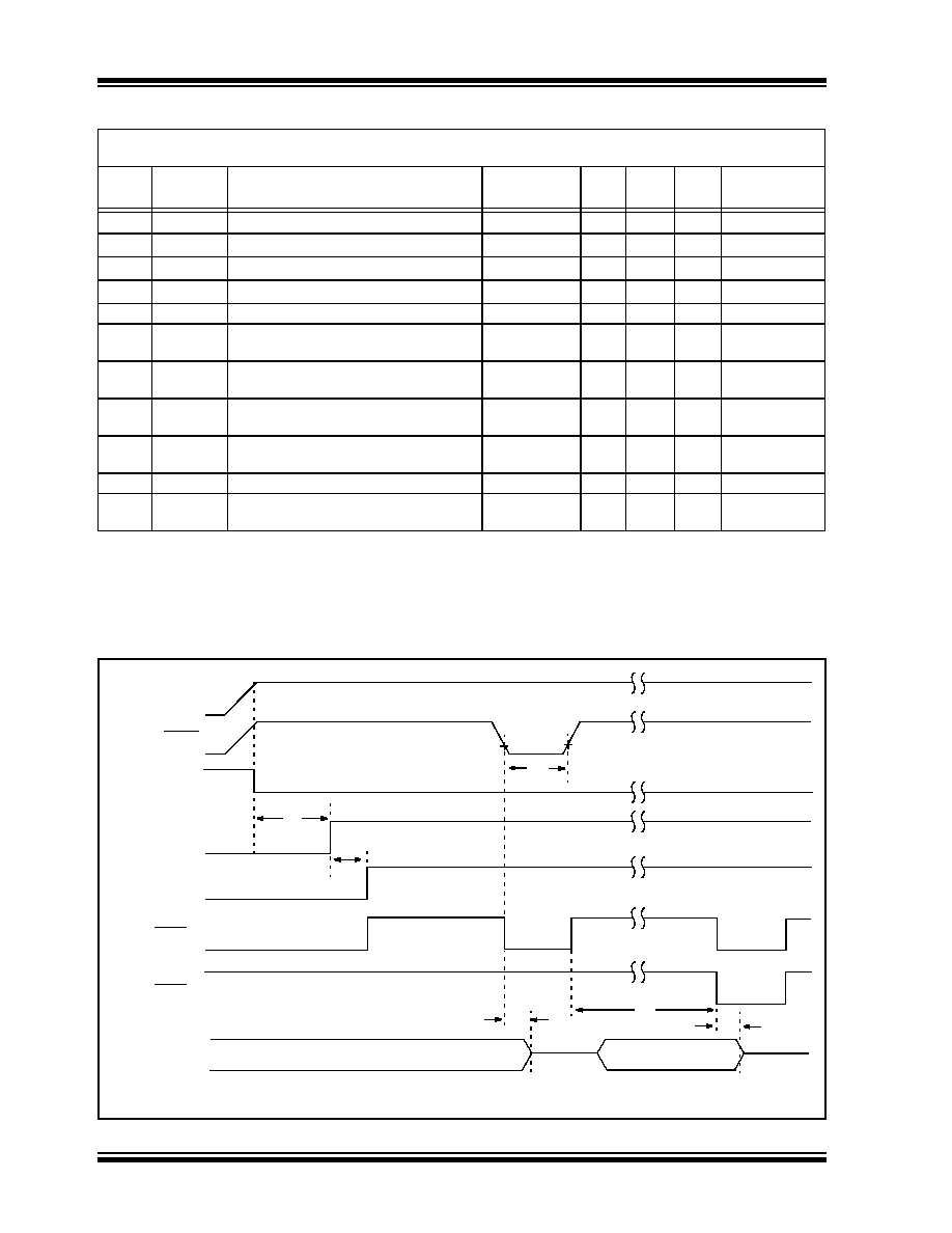
FIGURE 23-8:
RESET, WATCHDOG TIMER, OSCILLATOR START-UP TIMER AND POWER-UP
TIMER TIMING
Standard Operating Conditions (unless otherwise stated)
Operating Temperature -40°C
TA +125°C
Param
No.
Sym.
Characteristic
Min.
Typ Max. Units
Conditions
OS11
TosH2ckL Fosc
to CLKOUT (1)
——
70
ns
VDD = 3.3-5.0V
OS12
TosH2ckH Fosc
to CLKOUT (1)
——
72
ns
VDD = 3.3-5.0V
OS13
TckL2ioV
CLKOUT
to Port out valid(1)
——
20
ns
OS14
TioV2ckH
Port input valid before CLKOUT
(1)
TOSC + 200 ns
—
ns
OS15
TosH2ioV
Fosc
(Q1 cycle) to Port out valid
—
50
70*
ns
VDD = 3.3-5.0V
OS16
TosH2ioI
Fosc
(Q2 cycle) to Port input invalid
(I/O in hold time)
50
—
ns
VDD = 3.3-5.0V
OS17
TioV2osH Port input valid to Fosc
(Q2 cycle)
(I/O in setup time)
20
—
ns
OS18
TioR
Port output rise time(2)
—
40
15
72
32
ns
VDD = 2.0V
VDD = 3.3-5.0V
OS19
TioF
Port output fall time(2)
—
28
15
55
30
ns
VDD = 2.0V
VDD = 3.3-5.0V
OS20* Tinp
INT pin input high or low time
25
—
ns
OS21* Trbp
PORTB interrupt-on-change new input
level time
TCY
——
ns
*
These parameters are characterized but not tested.
Data in “Typ” column is at 3.0V, 25
C unless otherwise stated.
Note 1: Measurements are taken in RC mode where CLKOUT output is 4 x TOSC.
2: Includes OSC2 in CLKOUT mode.
VDD
MCLR
Internal
POR
PWRT
Time-out
OSC
Start-Up Time
Internal Reset(1)
Watchdog Timer
33
32
30
31
34
I/O pins
34
Note 1: Asserted low.
Reset(1)
发布紧急采购,3分钟左右您将得到回复。
相关PDF资料
PIC12C508A-04/SN
IC MCU OTP 512X12 8SOIC
PIC12C509A-04/SM
IC MCU OTP 1KX12 8-SOIJ
PIC16LF627T-04I/SO
IC MCU FLASH 1KX14 COMP 18SOIC
PIC12C509A-04/P
IC MCU OTP 1KX12 8DIP
PIC18LC452T-I/PT
IC MCU OTP 16KX16 A/D 44TQFP
PIC12LF1822-I/MF
IC MCU 8BIT FLASH 8DFN
PIC12F1822-I/P
IC MCU 8BIT FLASH 8PDIP
PIC12F1822-I/MF
IC MCU 8BIT FLASH 8DFN
相关代理商/技术参数
PIC16F723AT-I/ML
功能描述:8位微控制器 -MCU 7KB Flash 1.8V-5.5V. 16 MHz int Osc RoHS:否 制造商:Silicon Labs 核心:8051 处理器系列:C8051F39x 数据总线宽度:8 bit 最大时钟频率:50 MHz 程序存储器大小:16 KB 数据 RAM 大小:1 KB 片上 ADC:Yes 工作电源电压:1.8 V to 3.6 V 工作温度范围:- 40 C to + 105 C 封装 / 箱体:QFN-20 安装风格:SMD/SMT
PIC16F723AT-I/MV
功能描述:8位微控制器 -MCU 7KB Flash 1.8V-5.5V. 16 MHz int Osc RoHS:否 制造商:Silicon Labs 核心:8051 处理器系列:C8051F39x 数据总线宽度:8 bit 最大时钟频率:50 MHz 程序存储器大小:16 KB 数据 RAM 大小:1 KB 片上 ADC:Yes 工作电源电压:1.8 V to 3.6 V 工作温度范围:- 40 C to + 105 C 封装 / 箱体:QFN-20 安装风格:SMD/SMT
PIC16F723AT-I/SO
功能描述:8位微控制器 -MCU 7KB Flash 1.8V-5.5V. 16 MHz int Osc RoHS:否 制造商:Silicon Labs 核心:8051 处理器系列:C8051F39x 数据总线宽度:8 bit 最大时钟频率:50 MHz 程序存储器大小:16 KB 数据 RAM 大小:1 KB 片上 ADC:Yes 工作电源电压:1.8 V to 3.6 V 工作温度范围:- 40 C to + 105 C 封装 / 箱体:QFN-20 安装风格:SMD/SMT
PIC16F723AT-I/SS
功能描述:8位微控制器 -MCU 7KB Flash 1.8V-5.5V. 16 MHz int Osc RoHS:否 制造商:Silicon Labs 核心:8051 处理器系列:C8051F39x 数据总线宽度:8 bit 最大时钟频率:50 MHz 程序存储器大小:16 KB 数据 RAM 大小:1 KB 片上 ADC:Yes 工作电源电压:1.8 V to 3.6 V 工作温度范围:- 40 C to + 105 C 封装 / 箱体:QFN-20 安装风格:SMD/SMT
PIC16F723-E/ML
功能描述:8位微控制器 -MCU 7 KB Flash 18V-55V 16 MHz Int Osc RoHS:否 制造商:Silicon Labs 核心:8051 处理器系列:C8051F39x 数据总线宽度:8 bit 最大时钟频率:50 MHz 程序存储器大小:16 KB 数据 RAM 大小:1 KB 片上 ADC:Yes 工作电源电压:1.8 V to 3.6 V 工作温度范围:- 40 C to + 105 C 封装 / 箱体:QFN-20 安装风格:SMD/SMT
PIC16F723-E/MV
功能描述:8位微控制器 -MCU 7KB Flash 1.8V-5.5V RoHS:否 制造商:Silicon Labs 核心:8051 处理器系列:C8051F39x 数据总线宽度:8 bit 最大时钟频率:50 MHz 程序存储器大小:16 KB 数据 RAM 大小:1 KB 片上 ADC:Yes 工作电源电压:1.8 V to 3.6 V 工作温度范围:- 40 C to + 105 C 封装 / 箱体:QFN-20 安装风格:SMD/SMT
PIC16F723-E/SO
功能描述:8位微控制器 -MCU 7 KB Flash 18V-55V 16 MHz Int Osc RoHS:否 制造商:Silicon Labs 核心:8051 处理器系列:C8051F39x 数据总线宽度:8 bit 最大时钟频率:50 MHz 程序存储器大小:16 KB 数据 RAM 大小:1 KB 片上 ADC:Yes 工作电源电压:1.8 V to 3.6 V 工作温度范围:- 40 C to + 105 C 封装 / 箱体:QFN-20 安装风格:SMD/SMT
PIC16F723-E/SP
功能描述:8位微控制器 -MCU 7 KB Flash 18V-55V 16 MHz Int Osc RoHS:否 制造商:Silicon Labs 核心:8051 处理器系列:C8051F39x 数据总线宽度:8 bit 最大时钟频率:50 MHz 程序存储器大小:16 KB 数据 RAM 大小:1 KB 片上 ADC:Yes 工作电源电压:1.8 V to 3.6 V 工作温度范围:- 40 C to + 105 C 封装 / 箱体:QFN-20 安装风格:SMD/SMT